PCB Design &Product Engineeringin India

Indian hardware, designed in India. Our New Delhi team designs the board, writes the firmware and builds the Android app — planned for BIS and WPC approval and for manufacture with Indian EMS partners.

Board, firmware & app from one team · NDA before day one · You own every design file
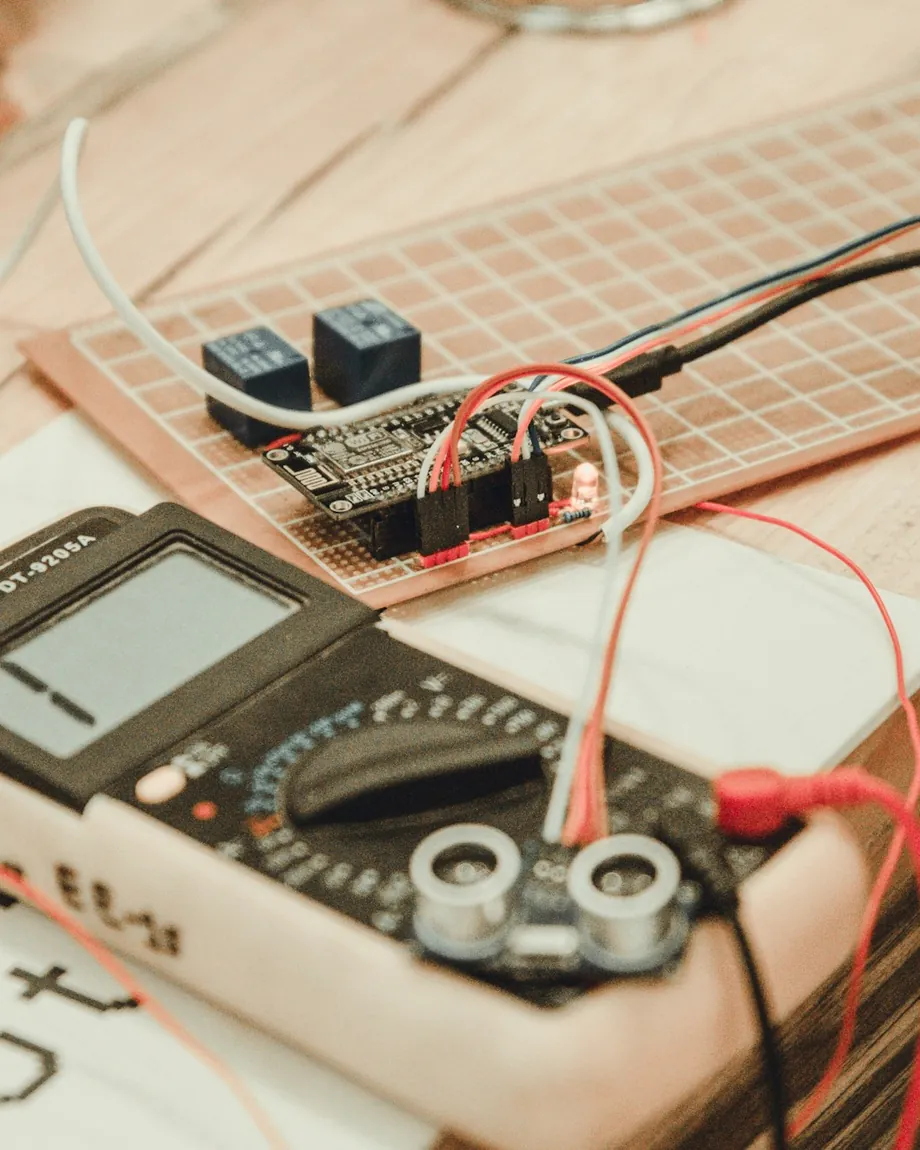
Testing an electronic circuit — PCB design company in India, Borgfy

First prototype in

4–8 wks

Hardware Design for India

India is building electronics at home faster than ever. Production-linked incentives and the Electronics Component Manufacturing Scheme are pulling component and assembly lines into the country, and EMS factories in Noida, Chennai, Bengaluru, Pune and Hyderabad can take a product from a first run to volume.

Our head office is in Vasant Kunj, New Delhi, so teams across Delhi NCR — Noida, Gurugram, Faridabad, Greater Noida — can meet us in person, and we work with founders and manufacturers everywhere else in India over video. We design around parts you can actually buy here, with second sources for anything that is slow to import.

Every design is planned for Indian approvals from day one: BIS registration for electronics, WPC Equipment Type Approval for anything with Wi-Fi or Bluetooth, and TEC testing where telecom rules apply — so the approval stage doesn't send you back to the drawing board.

Working with product teams in

  • New Delhi
  • Noida
  • Gurugram
  • Bengaluru
  • Chennai
  • Pune
  • Hyderabad
  • Ahmedabad
  • Mumbai

Approvals, Planned From Day One

We design for these rules from the first schematic and prepare the paperwork. Testing is done by an accredited lab, and we coordinate it for you.

BIS registration

Compulsory Registration Scheme for many electronic products — we design to the relevant IS standard and prepare the file for the lab.

WPC ETA

Equipment Type Approval for Wi-Fi, Bluetooth and other radios in de-licensed bands, filed through the Saral Sanchar portal.

TEC / MTCTE

Mandatory testing and certification for telecom and connected equipment where it applies to your product.

E-waste & RoHS

Restricted-substance limits under India's E-Waste Management Rules, met through the parts list.

Who We Build For in India

Make-in-India product companies

Replace imported boards with a design you own — lower landed cost, local supply and IP that stays with your company.

Hardware startups

Smart home, agritech, EV accessories and wearables — investor-ready prototypes, then a clean path to the first batch.

Factories going smart

Machine-monitoring sensors, energy meters and alerts sent to WhatsApp — retrofitted to the machines you already run.

Everything From Board to App

Full Details

Ways to Work With Us

Start with the design, stop at a working prototype, or hand us the whole product. You own every file either way.

01

Design only

A complete, manufacturer-ready design package — schematics, layout, BOM and production files. Your team or factory takes it from there.

02

Design + prototype

We design, order, assemble and bring up the first boards, and hand you working units to test, demo and show investors.

03

Full product

Board, firmware, enclosure, app and cloud — carried through certification and the first production run with your manufacturer.

We Also Design Hardware For

Common Questions

Plain answers, no jargon.

Yes. We design around parts available in the Indian market and hand off to Indian EMS partners for prototype and production runs, or to the manufacturer you already use.

Most products with Wi-Fi or Bluetooth need WPC Equipment Type Approval, and many electronic products need BIS registration. We confirm what applies on the scoping call, design for it, and coordinate testing with an accredited lab.

Yes. Our head office is at Vasant Kunj, New Delhi, and we regularly meet clients across Delhi NCR. Teams elsewhere in India work with us over video and receive prototypes by courier.

A simple board can be designed in one to two weeks. A connected product with firmware usually reaches its first working prototype in four to eight weeks, including fabrication and assembly. Complex multilayer or certification-bound products take longer — you get a dated plan before any work starts.

You do. Schematics, PCB layout source files, Gerbers, BOM, firmware source code, enclosure CAD and app code are all handed over in your name, and we sign an NDA before you share anything.

A PRODUCT IDEA, OR A BOARD THAT NEEDS FIXING?

Tell us what it should do. We’ll plan the build.

Free 30-minute call · NDA first · Written scope within 24 hours